 The FPGA and CPLD devices were developed with the intent of achieving the circuit density and speed like ASIC (Application Specific Integrated Circuit) but with a smaller turn around time for the programmable devices. The main difference between the FPGA and CPLD is that FPGA provides extensive logic resources as compared to the CPLD, which is simple and contain less number of interconnections.
For segregating the FPGA and CPLD, mainly two things are considered. First, is their architecture and how the architecture implements the different logic functions. Secondly, the distinct semiconductor technology employed in the hardware.
Content: FPGA Vs CPLD
Comparison Chart
| Basis for comparison | FPGA | CPLD |
|---|---|---|
| Stands for | Field Programmable Gate Array | Complex Programming Logic Design |
| Ratio of flip-flops | More | Less |
| Structure resembles to | Gate array | PAL |
| Density | Medium to high | Low to medium |
| Speed | Can be anticipated | Solely depend upon the application |
| Interconnect | Crossbar | Routing |
| Power consumption | High | Medium |
| Based on | RAM | EEPROM |
| Cost | Expensive | Cheap |
| Volatility | Can experience loss of data when power is disconnected. | Power down does not result in the loss of data. |
Definition of FPGA
FPGA (Field Programmable Gate Arrays) is named so, because of its construction is similar to gate array ASIC (Application Specific Integrated Circuit). It is built as a circuit containing the matrix of gate array logic which can also be reconfigured. The configuration of the FPGA generates an impact on the hardware by the software implication due to the connection of the internal circuitry. FPGA does not require the same resource like processors as these work parallelly and this boost the performance of a portion of the application as the other part of the application will not affect it.
It also enables the execution of the multiple control loops at varying rates. Dissimilar to hardwired PCB (Printed Circuit Board), FPGA can rewire the entire internal circuits to enable the reconfiguration at the time of deployment of the hardware. The FPGA circuitries are reliable as a dedicated hardware circuitry.
FPGA Components
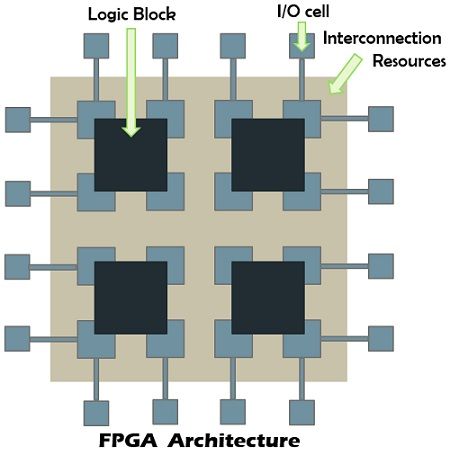
FPGA incorporate a large number of logic gates in one integrated circuit which makes it a good substitution for the numerous discrete components. The FPGA chip is comprised of a matrix of reconfigurable logic blocks as the internal resource enclosed by the I/O blocks, and the signals routing is done with the help of programmable interconnect switches and wire paths. It implements the multiple level low fan-in gates in the logic blocks rather than two-level AND and OR gates to make it denser.
Definition of CPLD
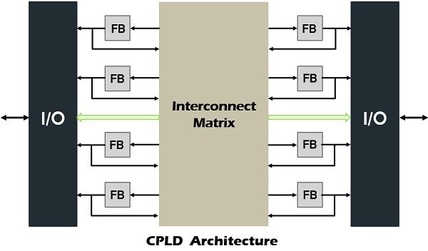
CPLD (Complex Programming Logic Devices) is a collection of multiple SPLD (Simple Programmable Logic Device) type of blocks incorporated on a single chip. It uses several PAL like blocks and programmable interconnection wires, which we have discussed in the previous article difference between PLA and PAL. The PAL is composed of AND and OR array where AND gate connections are fixed but OR gate connections are programmable. These PAL like blocks are linked to some input/output pins and are programmed with the help of the programming switches corresponding to interconnection wires (located horizontally and vertically).
CPLD Components
- A function block in CPLD contains the AND plane which can receive inputs from the I/O blocks, function blocks or response from the same function block. The terms are then inserted in the OR array and selected with the help of large multiplexer. The result of the MUX can be moved directly out of the block or via clocked flip-flop. This functional block can also have supplementary logic for example choosable exclusive OR, a master reset signal and ability to program the polarity at various stages.

- The I/O blocks are used for impelling the signals to the CPLD pins at the suitable voltage level and current. This facilitates in the elimination of the delay, reduction of the device hold time requirement and an addition of the more resources to the device.
- Interconnect in a CPLD is a huge matrix of programmable switch that directs the movement of the signals from one to another part of the device.
- It also uses programmable components such as PROM, EPROM, EEPROM and flash EPROM.
Key Differences Between FPGA and CPLD
- Ratio of flip-flops in FPGA is larger than the CPLD.
- The CPLD is similar to PAL while FPGA resembles Gate array.
- FPGA technology is denser than CPLD.
- The FPGA works in a faster manner, and its speed is predictable. On the contrary, the speed of CPLD entirely depends on the application it is used for.
- When it comes to power consumption, FPGA is ahead of CPLD.
- FPGA is based on RAM that is the reason it is volatile. As against, CPLD uses ROM variant as the programmable elements.
- FPGA is costlier as compared to CPLD.
Conclusion
The FGPAs provides higher complexity, flexibility, features like on-chip RAM, clock management, DSP functions, multipliers and so on. However, the power consumption in CPLD is less than FPGA. FPGA devices are more likely used in the designs where the changes are frequently applied, whereas CPLD used in situations where simple glue-logic is needed and when instant-on circuits are required for the application as initially FPGA functions at a slower speed cause because of the loading of configuration from the external ROM.
Leave a Reply